- 您现在的位置:买卖IC网 > Sheet目录329 > IDT70T653MS12BCI (IDT, Integrated Device Technology Inc)IC SRAM 18MBIT 12NS 256BGA
IDT70T653M
High-Speed 2.5V 512K x 36 Asynchronous Dual-Port Static RAM
Industrial and Commercial Temperature Ranges
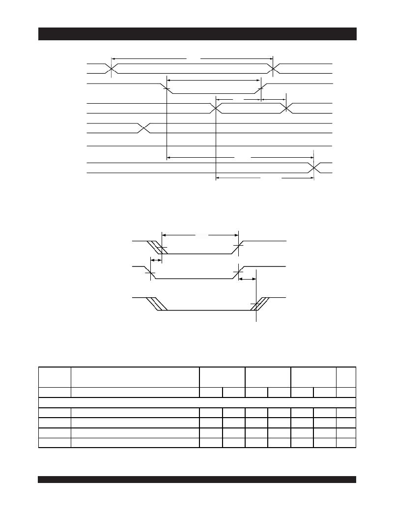
Timing Waveform of Write with Port-to-Port Read (1,3)
t WC
ADDR "A"
MATCH
t WP
R/ W "A"
DATA IN "A"
t DW
VALID
t DH
ADDR "B"
MATCH
(4)
R/ W "B"
t WDD
DATA OUT "B"
VALID
NOTES:
1. CE 0L = CE 0R = V IL ; CE 1L = CE 1R = V IH .
t DDD (3)
5679 drw 14a
.
2. OE = V IL for the reading port.
3. All timing is the same for left and right ports. Port "A" may be either the left or right port. Port "B" is the port opposite from port "A".
4. R/ W B = V IH .
Timing Waveform of Write with BUSY
t WP
R/ W "A"
t WB
BUSY "B"
R/ W "B"
(2)
t WH (1)
NOTES:
1. t WH must be met for BUSY input.
2. BUSY is asserted on port "B" blocking R/ W "B" , until BUSY "B" goes HIGH.
AC Electrical Characteristics Over the
Operating Temperature and Supply Voltage Range (1,2)
5679 drw 15
.
70T653MS10
Com'l Only
70T653MS12
Com'l
& Ind
70T653MS15
Com'l Only
Symbol
Parameter
Min.
Max.
Min.
Max.
Min.
Max.
Unit
INTERRUPT TIMING
t AS
t WR
t INS
t INR
Address Set-up Time
Write Recovery Time
Interrupt Set Time
Interrupt Reset Time
0
0
____
____
____
____
10
10
0
0
____
____
____
____
12
12
0
0
____
____
____
____
15
15
ns
ns
ns
ns
NOTES:
1. Timing is the same for both ports.
2. These values are valid regardless of the power supply level selected for I/O and control signals (3.3V/2.5V). See page 6 for details.
16
5679 tbl 16
发布紧急采购,3分钟左右您将得到回复。
相关PDF资料
IDT70V05L55G
IC SRAM 64KBIT 55NS 68PGA
IDT70V06L55G
IC SRAM 128KBIT 55NS 68PGA
IDT70V07L35G
IC SRAM 256KBIT 35NS 68PGA
IDT70V08S15PF
IC SRAM 512KBIT 15NS 100TQFP
IDT70V09L20PFI
IC SRAM 1MBIT 20NS 100TQFP
IDT70V18L20PFI
IC SRAM 576KBIT 20NS 100TQFP
IDT70V25L55G
IC SRAM 128KBIT 55NS 84PGA
IDT70V261L25PFGI
IC SRAM 256KBIT 25NS 100TQFP
相关代理商/技术参数
IDT70T653MS12BCI8
功能描述:IC SRAM 18MBIT 12NS 256BGA RoHS:否 类别:集成电路 (IC) >> 存储器 系列:- 标准包装:3,000 系列:- 格式 - 存储器:EEPROMs - 串行 存储器类型:EEPROM 存储容量:8K (1K x 8) 速度:400kHz 接口:I²C,2 线串口 电源电压:1.7 V ~ 5.5 V 工作温度:-40°C ~ 85°C 封装/外壳:8-SOIC(0.154",3.90mm 宽) 供应商设备封装:8-SOIC 包装:带卷 (TR)
IDT70T653MS15BC
功能描述:IC SRAM 18MBIT 15NS 256BGA RoHS:否 类别:集成电路 (IC) >> 存储器 系列:- 标准包装:3,000 系列:- 格式 - 存储器:EEPROMs - 串行 存储器类型:EEPROM 存储容量:8K (1K x 8) 速度:400kHz 接口:I²C,2 线串口 电源电压:1.7 V ~ 5.5 V 工作温度:-40°C ~ 85°C 封装/外壳:8-SOIC(0.154",3.90mm 宽) 供应商设备封装:8-SOIC 包装:带卷 (TR)
IDT70T653MS15BC8
功能描述:IC SRAM 18MBIT 15NS 256BGA RoHS:否 类别:集成电路 (IC) >> 存储器 系列:- 标准包装:3,000 系列:- 格式 - 存储器:EEPROMs - 串行 存储器类型:EEPROM 存储容量:8K (1K x 8) 速度:400kHz 接口:I²C,2 线串口 电源电压:1.7 V ~ 5.5 V 工作温度:-40°C ~ 85°C 封装/外壳:8-SOIC(0.154",3.90mm 宽) 供应商设备封装:8-SOIC 包装:带卷 (TR)
IDT70T659S10BC
功能描述:IC SRAM 4MBIT 10NS 256BGA RoHS:否 类别:集成电路 (IC) >> 存储器 系列:- 标准包装:3,000 系列:- 格式 - 存储器:EEPROMs - 串行 存储器类型:EEPROM 存储容量:8K (1K x 8) 速度:400kHz 接口:I²C,2 线串口 电源电压:1.7 V ~ 5.5 V 工作温度:-40°C ~ 85°C 封装/外壳:8-SOIC(0.154",3.90mm 宽) 供应商设备封装:8-SOIC 包装:带卷 (TR)
IDT70T659S10BC8
功能描述:IC SRAM 4MBIT 10NS 256BGA RoHS:否 类别:集成电路 (IC) >> 存储器 系列:- 标准包装:3,000 系列:- 格式 - 存储器:EEPROMs - 串行 存储器类型:EEPROM 存储容量:8K (1K x 8) 速度:400kHz 接口:I²C,2 线串口 电源电压:1.7 V ~ 5.5 V 工作温度:-40°C ~ 85°C 封装/外壳:8-SOIC(0.154",3.90mm 宽) 供应商设备封装:8-SOIC 包装:带卷 (TR)
IDT70T659S10BCI
功能描述:IC SRAM 4MBIT 10NS 256BGA RoHS:否 类别:集成电路 (IC) >> 存储器 系列:- 标准包装:3,000 系列:- 格式 - 存储器:EEPROMs - 串行 存储器类型:EEPROM 存储容量:8K (1K x 8) 速度:400kHz 接口:I²C,2 线串口 电源电压:1.7 V ~ 5.5 V 工作温度:-40°C ~ 85°C 封装/外壳:8-SOIC(0.154",3.90mm 宽) 供应商设备封装:8-SOIC 包装:带卷 (TR)
IDT70T659S10BCI8
功能描述:IC SRAM 4MBIT 10NS 256BGA RoHS:否 类别:集成电路 (IC) >> 存储器 系列:- 标准包装:3,000 系列:- 格式 - 存储器:EEPROMs - 串行 存储器类型:EEPROM 存储容量:8K (1K x 8) 速度:400kHz 接口:I²C,2 线串口 电源电压:1.7 V ~ 5.5 V 工作温度:-40°C ~ 85°C 封装/外壳:8-SOIC(0.154",3.90mm 宽) 供应商设备封装:8-SOIC 包装:带卷 (TR)
IDT70T659S10BF
功能描述:IC SRAM 4MBIT 10NS 208FBGA RoHS:否 类别:集成电路 (IC) >> 存储器 系列:- 标准包装:3,000 系列:- 格式 - 存储器:EEPROMs - 串行 存储器类型:EEPROM 存储容量:8K (1K x 8) 速度:400kHz 接口:I²C,2 线串口 电源电压:1.7 V ~ 5.5 V 工作温度:-40°C ~ 85°C 封装/外壳:8-SOIC(0.154",3.90mm 宽) 供应商设备封装:8-SOIC 包装:带卷 (TR)
